|
On this page ...
|
This serie of pages on this website will help you on your way with
the Parallax
(OEM) Basic Stamp II microcontroller.
On this page you will find a brief instruction on how to assemble
the Parallax OEM Basic Stamp II.
Keep in mind that this is a VERY brief instruction based on my personal
experiences. Read the disclaimer!
Tip: You can also consider building
your own HomeBrew
Basic Stamp! |
|
Before you start
When building the OEM Basic Stamp II kit, you should
ALWAYS follow the instructions that came with the kit. This can be either
a booklet or a CD-Rom.
In case you have only a CD-Rom, then it's adviseable
to either use the Parallax navigator (in the root of the CD-Rom: Welcome.exe
- which autoruns if autorun is enabled on your PC).
If you do not want to use this navigator, then please
take a look at the Adobe
Acrobat document called OEM_BS2_Manual.PDF
in the directory \Documentation\Basic_Stamps\OEM_BS2
(relative to the root of the CD-Rom).
Adobe Acrobat can be found on the CD-Rom in the directory
\Acrobat Reader or
at the Adobe website.
In order to avoid problems ...
Onces you start building, keep these tips in mind to
avoid or limit confusion and trouble:
- Orientation of the Resistor networks
The dot, found on the resitor network end, should be pointing to the
markings on the PCB "RN1" and "RN2".
The manual mentions a pin identification but I could not find one on
my PCB. I'm not sure if this is what Parallax
had in mind, but anyway it worked for me (considering the setup of the
resistor networks it will probably not matter how you orientate them
anyway).
- Keep in mind that the 4 transistors are different!
- Q1 and Q2 are a 2N3904 (NPN)
- Q3 is a 2N3906 (PNP)
- U3 is a MN13811 (Reset Supervisor)
- Powersupply
I used a simple powersupply that is already regulated to 5V.
Make sure youconnect:
+5V to Vin
GND to Vss
The purpose of Vdd is that if there is power available on the PCB this
pin will output +5V as regulated by the LM2940 power regulator. You
could use this to hookup a LED (Light Emitting Diode) to indicate that
the BASIC Stamp is powered.
- Do not overheat components
Avoid overheating by using proper soldering equipment. When mounting
the sockets for the chip do this without the chip inserted! First solder
the socket, once cooled down insert the chip.
- Bending the pins of the 2 chips
You might need to bend the legs of the chip a bit to get it fitted smoothly,
this is how to do that:
Press one side of the chip gently on a flat surface, this way the pins
on one side of the chip are bend equally. Repeat this for the otherside
too. Remember to do this GENTLY.
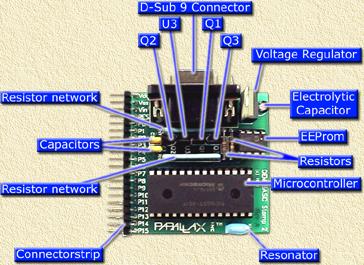
Assembly Steps
Follow these steps to assemble your OEM Basic Stamp II (revision A based
- other versions might slightly differ), and take a good look at this
picture to get an idea where to put the items:
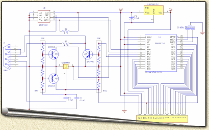
For the more experienced users, here you see the scematics
of the OEM Basic Stamp II (click to enlarge):
1.
|
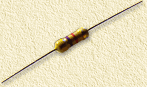
RESISTORS
The resistors used are 4.7K Ohm (Yellow, Purple, Red - and Gold
band). Resistors are polarity insensitive, which means that it doesn’t
matter which end goes where. Install the resistors on the PCB identified
by "R1" and "R2".
|
|
| 2. |
CONNECTOR STRIP
The side with the bend pins should be inserted into the pcb. Install
the strip header on the PCB identified by "X1".
|
|
| 3. |
CAPACITORS
Two 0.1 uF ceramic capacitors (little brown components with 2 pins)
are used. Like, the resistors, it doesn’t matter which way
these are installed. Install the two capacitors on the PCB identified
by "C2" and "C3".
|
|
| 3. |
RESISTOR NETWORKS
The resistor networks look like little blue mini combs. The dot,
found on the resitor network end, should be pointing to the markings
"RN1" and "RN2" on the PCB.
|
|
| 4. |
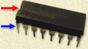
CHIP/IC and their SOCKETS
Nearly all ICs have a ‘Pin 1’ marker, that denotes
the location of Pin 1. It is important to install chips with the
proper orientation!
In the image on the right, the red arrow indicates the orientation
notch. The blue arrow indicates pin 1.
To make things a bit easier: For the IC sockets that you will be
installing, there is a notch along the outside edge of the board
on one of the short sides. Match this notch with the notch printed
on the PCB on the locations "U1" and "U2".
|
 |
| 5. |
RESONATOR or X-TAL
The ceramic resonator, a brown or blue component with 3 pins, is
polarity insensitive. It doesn’t matter which way it is installed,
it will still work OK. Install the ceramic resonator on the PCB
at the location called "XTAL".
(not to be confused with X1!)
|
|
| 6. |
ELECTROLYTIC CAPACITOR
The electrolytic capacitor looks like a small cylinder with two
long pins on one end. The electrolytic capacitor will have the negative
lead marked with one or more ‘-’ signs. Install the leg
NOT marked with the ‘-’ signs in the hole closest to the
‘+’ sign in the "C1" space on the PCB.
|
|
| 7. |
TRANSISTOREN
- First install the Reset Supervisor; it looks like a black knop
with three legs and bears the mark, "13811". The
white silkscreen on the pcb will guide you as to how to orient this
component ("U3"). You will need to bend the middle
pin slightly to get it to fit.
- There are three other components that closely resemble the Reset
Supervisor. Two of these have the same marking "3904"
and should be placed on "Q1" and "Q2"
on the PCB. For these two to fit you will need to bend the middle
pin too.
- The last remaining look-a-like is "Q3", marked
"3906". Install this transistor in a similar fashion
on location "Q3".
|
|
| 8. |
D-SUB 9 CONNECTOR
Now install the 9-pin D-Sub connector. This looks like it will
plug into a serial cable. There is no way to plug in backwards.
|
|
| 9. |
VOLTAGE REGULATOR (Spanningsregelaar)
The last component to solder on is the voltage regulator, "VR1".
It is a black plastic square with a metal tab protruding from the
top. Install this with the metal tab closest to the 9-pin D-Sub
connector. This component is polarity sensitive and MUST be installed
correctly.
The voltage regulator makes sure the power supplied to the Basic-Stamp
is not exceeding the 5V limit.
|
|
|